
Certain elements and their solid state crystals are classified as conductors, semiconductors or insulators depending on their relative ability to carry electric current. As seen in the structure of an atom, there is valence band. There is energy gap region between this band and the conduction band. When some outside influence such as an electric field or heat is applied, a valence electron may acquire energy sufficient enough to jump through the forbidden energy gap and pass on into conduction band of energy. In conductors there is no gap between the valence band and the conduction band. In insulators the energy gap is very wide. Semiconductors are neither good conductors nor insulators at normal room temperature. The conductivity of semiconductors lies between good conductors and good insulators e.g. the conductivity copper is 5.8 × 10⁷ mho/meter. The conductivity of semiconductors is in the range of 10-3 to 105 mho/m at 300°K, while insulators like quartz have conductivity as low as 10-16 mho/m. The energy required for the conductors to overcome the forbidden energy gap is very small e. g. 0.05 eV while for insulators it is many eV. For Silicon and Germanium (semiconductors) it is only 1.1 eV and 0.7 eV respectively.
The semiconductors in their pure form are called ‘intrinsic semiconductors’. The conductivity of semiconductors is increased many times by adding some quantity of other material called ‘impurity’. When the semiconductors have the added impurity they are known as ‘extrinsic semiconductors’. Impurity atoms are added to intrinsic germanium to make the crystal contain either extra electrons as charge carriers or extra holes as charge carriers. An impurity which provides extra electrons is called a donor element and an impurity which provides extra holes is called an acceptor element. Donor and acceptor elements are chosen from materials whose atoms have 5 and 3 valence electrons respectively. A semiconductor which has predominantly donor impurities is called an ‘N’ type semiconductor; while the semiconductor which has predominantly acceptor impurities is known as ‘P’ type semiconductor. N signifies the negative charge of loosely bound electrons in the material while P signifies the positive charges or holes in the material. In ‘P’ type semiconductors, impurity atoms used are Boron, Aluminum, Indium or Gallium having a valency of 3 while in ‘N’ type semiconductors atoms used are Arsenic, Antimony or Phosphorus having a valency of 5. If impurity atom such as Indium is added to Germanium atom, Indium has one electron short for completion of covalent bond. Hence it takes up one electron from the neighboring Germanium atom. This action creates a vacancy in the adjacent covalent bond and is called ‘hole’. This ‘hole’ may be filled by another electron from neighboring covalent bond. The holes being available increase the conductivity of the pure semiconductor and is known as ‘P’ type semiconductor. If Arsenic atom is added to the Germanium atom, there is one electron in excess of that required for completion of covalent bond. This extra electron is available as charge carrier. The conductivity of the semiconductor is increased by the addition of this impurity and is known as ‘N’ type semiconductor.
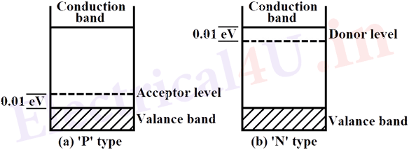
The addition of acceptor impurity introduces an energy state at 0.01eV above the top of the valence band of intrinsic semiconductor. The holes are ‘Majority’ carriers and electrons are ‘Minority’ carriers in ‘P’ type semiconductors. The addition of donor impurity introduces an energy state at 0.01eV below the bottom of the conduction band of the intrinsic semiconductor. In ‘N’ type semiconductor, electrons are ‘Majority’ charge carriers and holes are ‘Minority’ charge carriers. The energy band diagrams for ‘P’ type and ‘N’ type semiconductors are shown in Fig. 1 (a) and (b).